Lithography process development
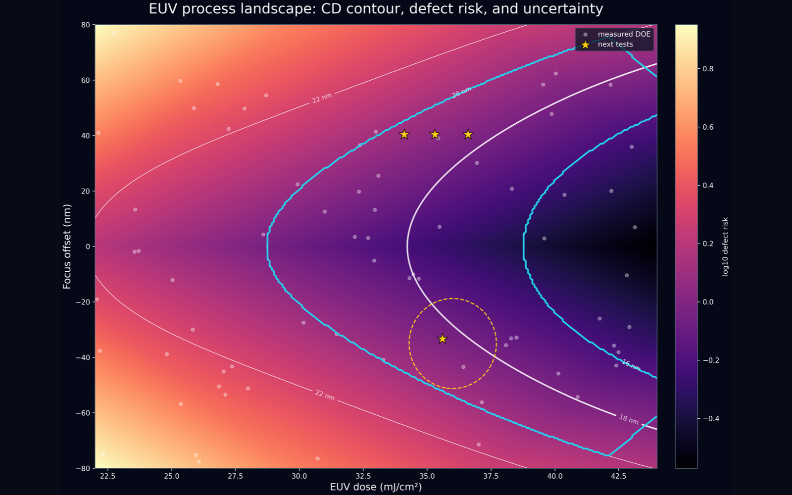
Analyze focus-exposure matrices, Bossung curves, process windows, CD response, stochastic variability, and next DOE points.
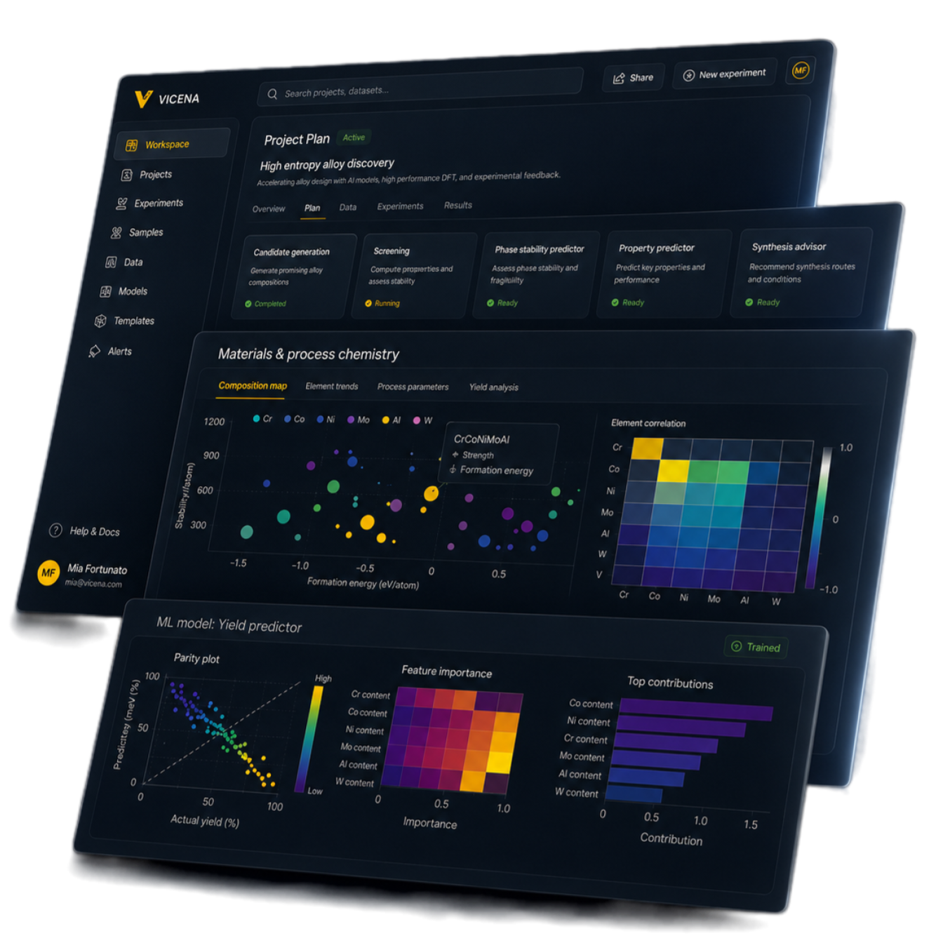
Vicena helps semiconductor scientists and engineers move from literature and IP research to material scouting, experiment design, simulation, data analysis, and decision-ready reports inside one deployable scientific workspace.
Literature + IP
Notebooks + data
Private deployment
Turn early technical questions into cited literature briefs, patent landscapes, material comparisons, and open-question lists.
Convert evidence and hypotheses into DOE tables, metrology plans, controls, acceptance criteria, and next-test recommendations.
Use reproducible notebooks for process windows, wafer maps, defect metrics, surrogate models, and data analysis that can be inspected later.
Generate technical briefs, CSV tables, figures, notebooks, compatibility memos, method drafts, and review-ready reports.
Why this matters
A semiconductor project rarely starts with one dataset. It starts with questions about materials, process windows, patents, tool time, simulation assumptions, metrology exports, and the next experiment. Vicena brings those steps into one traceable workspace.
01
Idea
02
Literature
03
IP
04
Materials
05
Experiment
06
Simulation
07
Data
08
Report
Semiconductor workflows
Use Vicena to keep the question, evidence, assumptions, files, simulations, data, and reports connected as the work moves from concept to experiment.
Analyze focus-exposure matrices, Bossung curves, process windows, CD response, stochastic variability, and next DOE points.
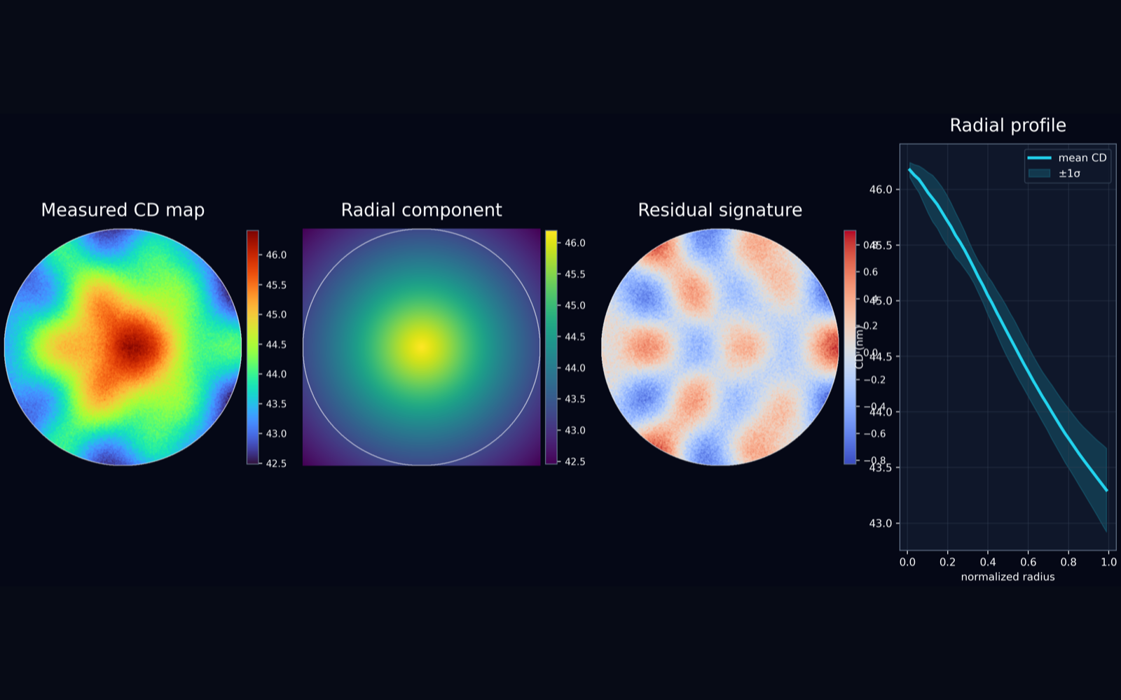
Decompose wafer-level signatures into radial trends, residuals, field effects, outliers, CDU, overlay, film thickness, and defect distributions.
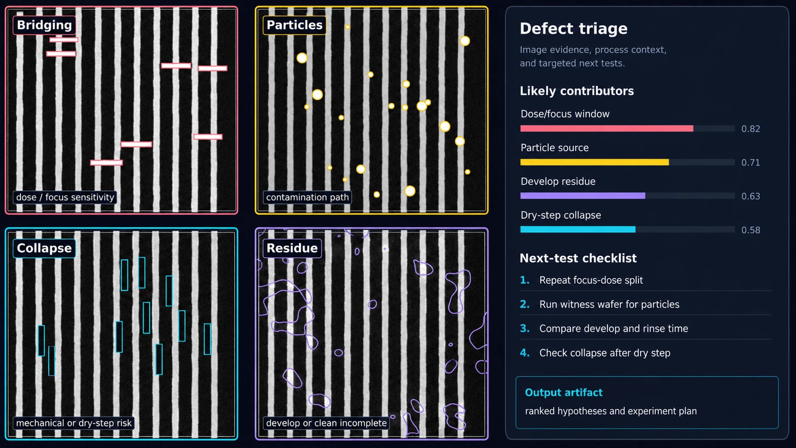
Cluster defect morphologies, connect process changes to failure hypotheses, and produce targeted next-test plans for review.
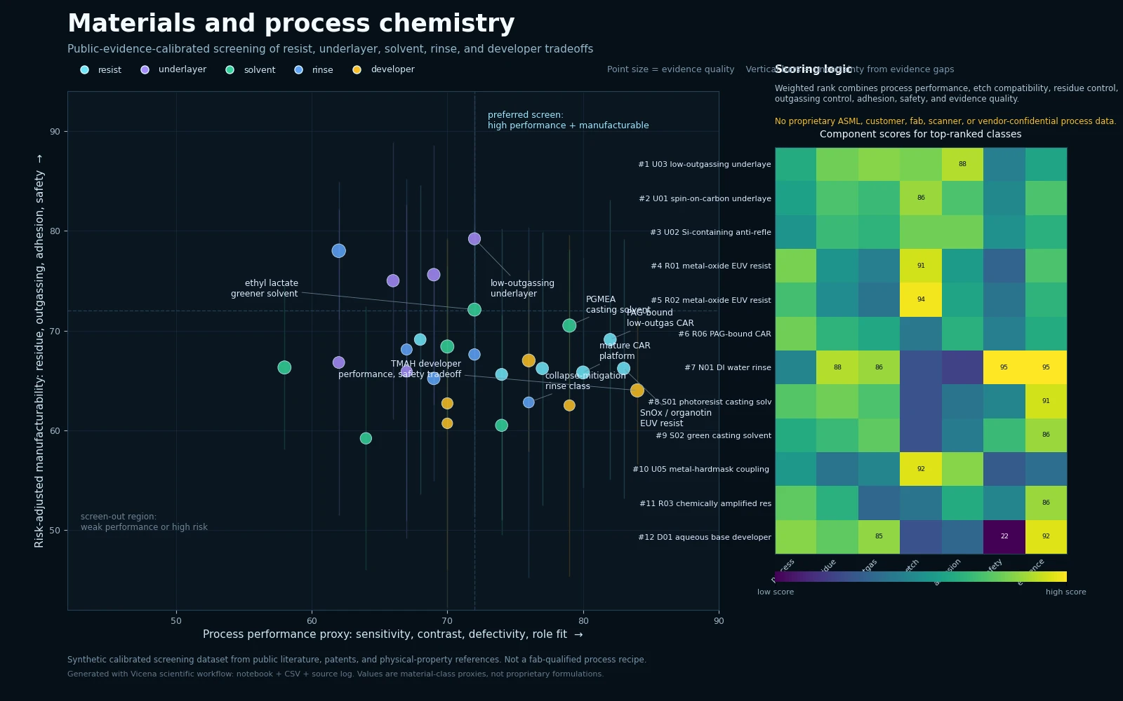
Screen candidates for compatibility, residue risk, outgassing concern, solubility, hazards, process performance, and supporting evidence.
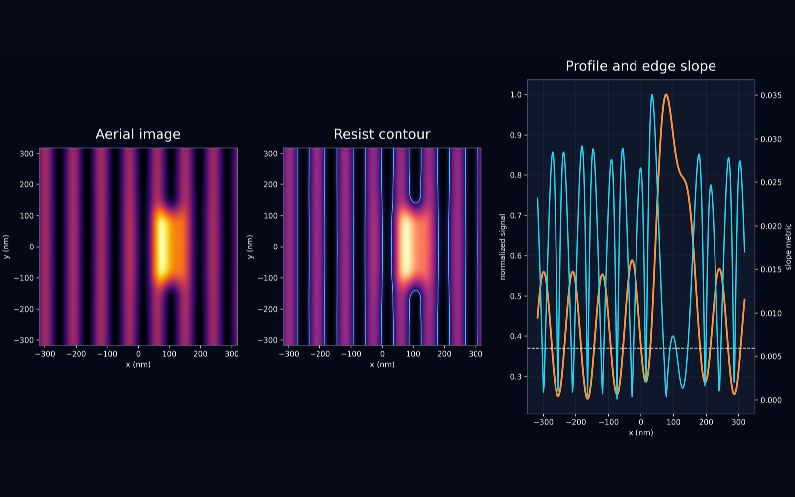
Explore how pattern geometry, source assumptions, threshold behavior, printed contours, and edge slope affect lithography decisions.
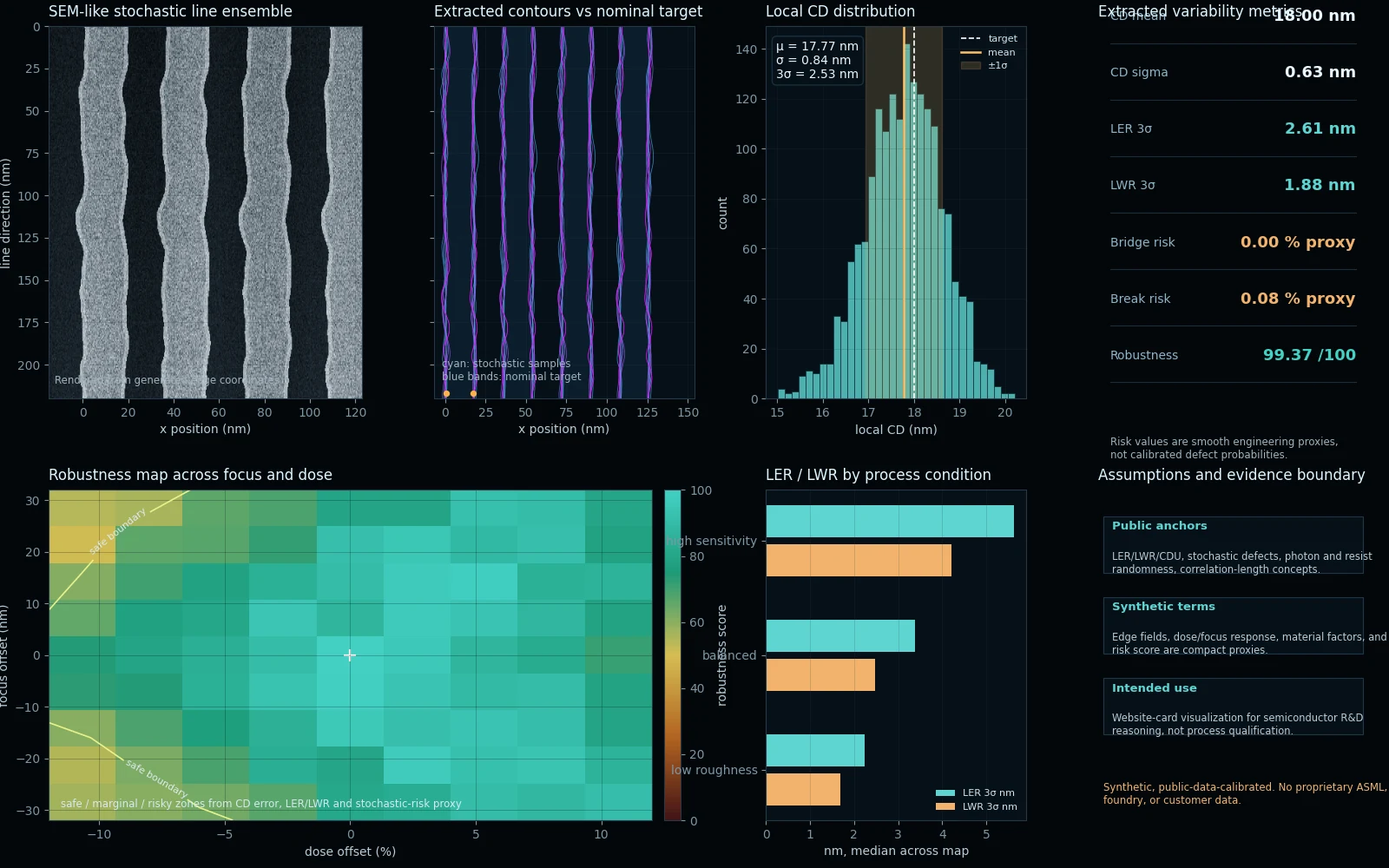
Visualize line-edge ensembles, CD distributions, process uncertainty, and robustness against focus, dose, and material variation.
Concrete outputs
Vicena combines AI reasoning with scientific work surfaces: workspace files, notebooks, literature and patent research, chemistry intelligence, method drafting, data analysis, and report generation.
Process-window notebook
DOE recommendation table
Wafer-map decomposition
Defect morphology embedding
Materials tradeoff map
Literature and patent brief
Compatibility memo
Method development protocol
Technical report
Control
Vicena can be used as a hosted scientific workspace or deployed where semiconductor teams need stronger data control. Enterprise deployments can connect AI to private files, experimental data, proprietary process models, internal archives, controlled compute, private model endpoints, and access-controlled workspaces.
Vicena supports technical landscape analysis and IP research workflows, but it does not provide legal freedom-to-operate conclusions. It is not positioned as a replacement for production OPC, scanner-control systems, TCAD, EDA, or calibrated lithography simulators.