
有公开服务证据
Center for Nanoscale Systems (CNS)
Center for Nanoscale Systems (CNS) at Harvard University provides shared-facility access for x-ray and synchrotron characterization, electron microscopy, nanofabrication and microfabrication, and optical microscopy and spectroscopy. Registration, training, project review, fees, and current instrument availability may apply.
公开提供对外服务
公开描述的能力
Advanced characterization
X-ray and synchrotron characterization
Advanced characterization
Electron microscopy
Fabrication
Nanofabrication and microfabrication
Advanced characterization
Optical microscopy and spectroscopy
Materials testing
Materials characterization
了解设备
仪器型号
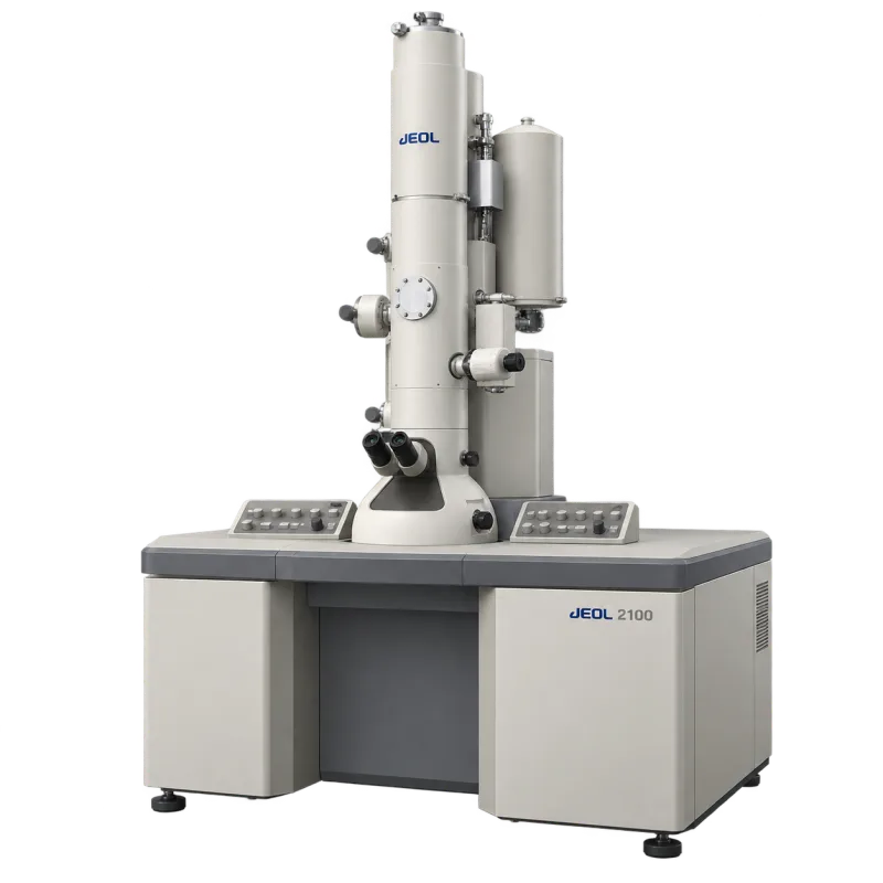
CAD 示意图展示的是仪器型号。实际安装配置和当前可用性需向实验室确认。
技术清单
技术与设备
-
表面分析
X-ray photoelectron spectroscopy instrumentation
-
实验室设备
atom probe tomography instrumentation
-
显微与成像
atomic force microscopy instrumentation
-
显微与成像
dual-beam FIB-SEM systems (two; model not stated on overview)
-
显微与成像
high-resolution scanning electron microscopes (three; model not stated on overview)
-
显微与成像
high-resolution transmission electron microscopes (four HRTEM systems; model not stated on overview)
-
光谱
Horiba LabRAM Evolution Raman system has 532 and 633 nm excitation, 800 mm spectrometer, 600/1800 gratings, Synapse CCD and confocal mapping.
-
显微与成像
JEOL 2100 is the standard self-use TEM after online, in-lab and one-on-one certification; advanced TEMs require additional training.
登记范围证据
- ◇Facility scope: Two-site shared-use facility with Cambridge nanofabrication and imaging/analysis plus Allston imaging/analysis and soft-lithography resources.
- ◇External access: Serves Harvard and the larger community of external academic and industry researchers.
- ◇Official-source, facility-specific instrument evidence is available. Current configuration, availability, price, and project fit require confirmation.
本条目依据的证据
这些公开条目由 Vicena 根据所引用的实验室来源整理。被收录不代表存在合作关系,也不代表目前可承接、已有报价或已接受项目。本主页不构成推荐、可用性确认或报价,也不代表存在商业合作关系。