
有公开服务证据
Cornell NanoScale Science & Technology Facility (CNF)
Cornell NanoScale Science & Technology Facility (CNF) at Cornell University provides shared-facility access for nanofabrication and microfabrication, surface and thin-film characterization, and optical microscopy and spectroscopy. Registration, training, project review, fees, and current instrument availability may apply.
公开提供对外服务
公开描述的能力
Fabrication
Nanofabrication and microfabrication
Advanced characterization
Surface and thin-film characterization
Advanced characterization
Optical microscopy and spectroscopy
了解设备
仪器型号
CAD 示意图展示的是仪器型号。实际安装配置和当前可用性需向实验室确认。
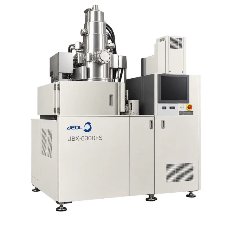 型号示意图
型号示意图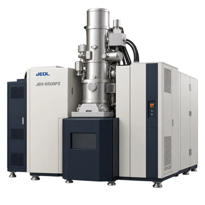 型号示意图
型号示意图技术清单
技术与设备
-
显微与成像
Bruker Dimension Icon atomic force microscope
-
微纳加工
JEOL JBX-6300FS electron-beam lithography system
-
微纳加工
JEOL JBX-9500FS electron-beam lithography system
-
实验室设备
Malvern NS300 NanoSight
-
实验室设备
Malvern Nano ZS Zetasizer
-
实验室设备
Nanonex NX-2500 nanoimprint system
-
实验室设备
Oxford FlexAL ALD system
-
显微与成像
Zeiss Gemini SEM
-
显微与成像
Zeiss Supra 55VP field-emission SEM
-
显微与成像
Zeiss Ultra 55 field-emission SEM
-
微纳加工
Cee Apogee resist spinners handle pieces through 200 mm wafers at more than 6000 rpm and up to 30000 rpm/s acceleration.
-
微纳加工
Disco DA810 grinder processes silicon, glass, sapphire, SiC and III-V workpieces to 8 inches; Disco dicing saw supports multiple substrate classes.
-
实验室设备
Finetech Fineplacer pico ma die bonder aligns chips to 20 x 20 mm over substrates to 100 x 100 mm with 5 micrometre placement accuracy and force to 20 N.
-
微纳加工
JEOL JBX-6300FS supports direct-write EBL on wafers to 150 mm with sub-10-nm capability.
-
微纳加工
JEOL JBX-9500FS EBL operates at 100 kV with 100 MHz clock and 1 x 1 mm write field, handling 10 mm pieces through 300 mm wafers and sub-10-nm features.
-
微纳加工
Oxford PlasmaPro 100 Cobra 300 ICP-RIE accepts 100, 150 and 200 mm wafers and provides 3 kW ICP source plus optical endpoint detection.
-
微纳加工
SUSS Gamma robotic coat/develop cluster handles wafer cassettes to 200 mm and includes AltaSpray for non-planar substrates.
登记范围证据
- ◇Access: Open user facility serving academic and company projects.
- ◇Commercial terms: Usage charged per hour by tool; industrial users pay market-equivalent rates.
- ◇Remote access: Some simple projects may be executed remotely by staff or independent contractors.
- ◇Official-source, facility-specific instrument evidence is available. Current configuration, availability, price, and project fit require confirmation.
本条目依据的证据
这些公开条目由 Vicena 根据所引用的实验室来源整理。被收录不代表存在合作关系,也不代表目前可承接、已有报价或已接受项目。本主页不构成推荐、可用性确认或报价,也不代表存在商业合作关系。