
← All labs

Public service evidence

Pritzker Nanofabrication Facility (PNF)

Pritzker Nanofabrication Facility (PNF) at University of Chicago provides shared-facility access for nanofabrication and microfabrication, and surface and thin-film characterization. Registration, training, project review, fees, and current instrument availability may apply.

External services publicly offered

2 capabilities 13 equipment records Reviewed 2026-08-29

Publicly described capabilities

Fabrication

Nanofabrication and microfabrication

Advanced characterization

Surface and thin-film characterization

Technical inventory

Techniques and equipment

3 equipment types
  • Microscopy & imaging

    SEM/AFM metrology equipment

  • Micro/nanofabrication

    cleanroom process equipment

  • Micro/nanofabrication

    electron-beam lithography system

  • Micro/nanofabrication

    photolithography system

  • Micro/nanofabrication

    plasma etching system

  • Micro/nanofabrication

    thin-film deposition system

  • Micro/nanofabrication

    AJA Orion sputtering, Angstrom EvoVac/Nexdep and Plassys MEB550S support sputter, e-beam, thermal and ion-assisted deposition.

  • Microscopy & imaging

    Bruker Dimension Icon AFM supports topography plus nanomechanical, nanoelectrical and nanoscale chemical mapping.

  • Laboratory equipment

    Cambridge Fiji G2 plasma ALD and Savannah ALD support thermal/plasma films and conformal coating of ultra-high-aspect-ratio substrates.

  • Microscopy & imaging

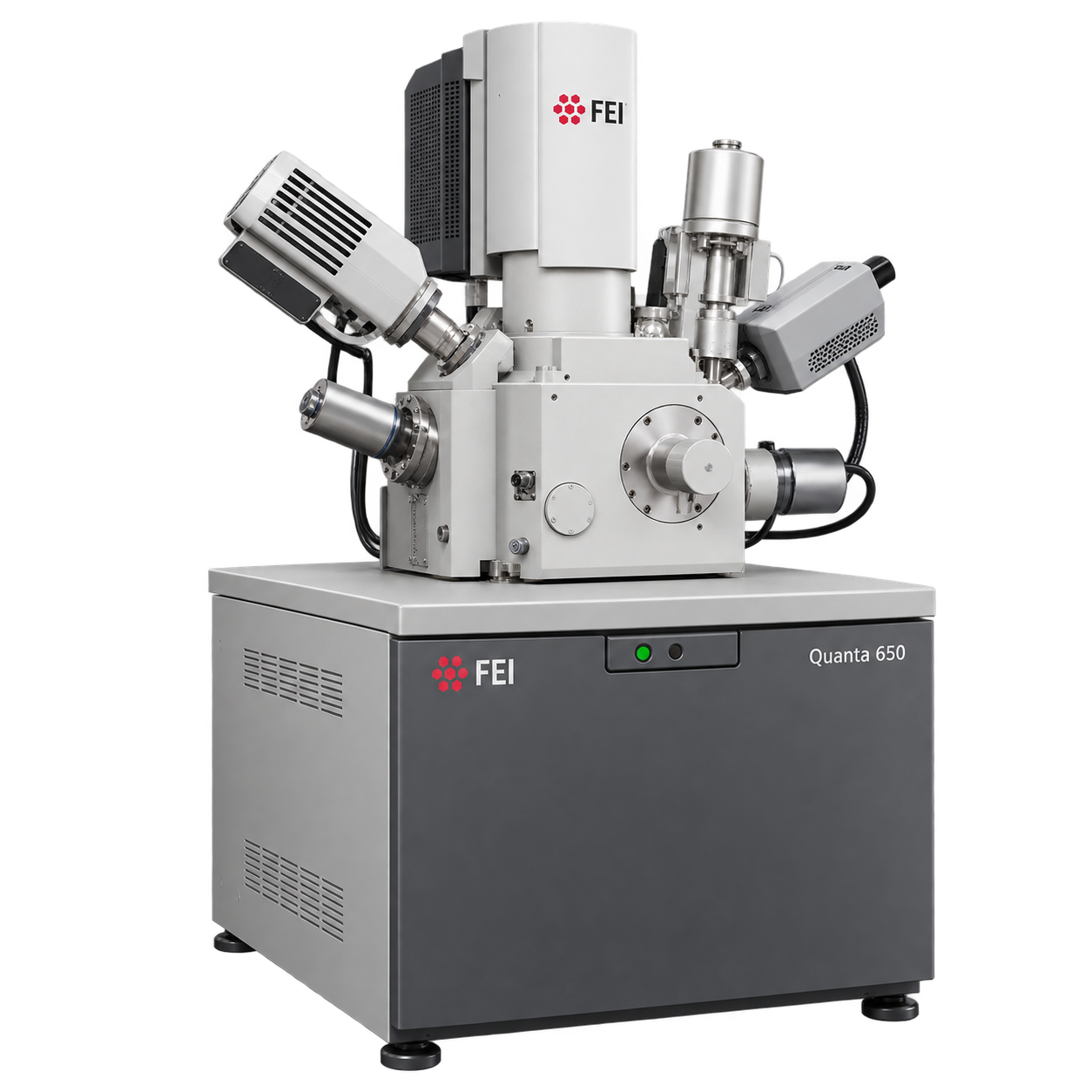
    FEI Quanta 650 FEG SEM has eight detectors, sub-5-nm imaging and Nabity NPGS electron-beam patterning.

  • Micro/nanofabrication

    Heidelberg MLA150 direct-write lithography provides maskless exposure, backside alignment and a 150 x 150 mm exposure area.

  • Micro/nanofabrication

    Plasma-Therm ICP chlorine/fluorine systems, Versaline deep-silicon RIE and Vision 310 PECVD support plasma processing.

  • Laboratory equipment

    Raith EBPG5200 electron-beam writer handles substrates and masks to 155 mm/6 inches, operates at 20, 50 or 100 kV and supports features below 8 nm.

Registry scope evidence

  • External access: Open to all properly trained users through a fee-for-use structure..
  • Facility: 10,000-square-foot ISO class 5 cleanroom supporting R&D and prototype production..
  • Capabilities: Lithography, deposition, plasma etching, microscopy and thin-film metrology are listed..
  • Address: Facility is in Eckhardt Research Center lower level 1..
  • Official-source, facility-specific instrument evidence is available. Current configuration, availability, price, and project fit require confirmation.

Evidence used for this listing

Vicena compiles these public listings from cited laboratory sources. A listing does not imply a partnership, current availability, pricing, or acceptance of a project. This profile is not an endorsement, availability check, quote, or representation of a commercial relationship.